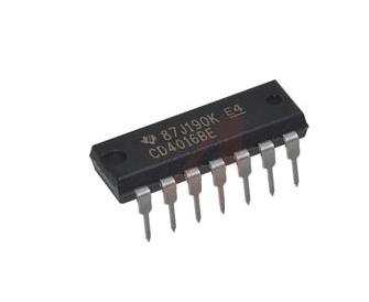
The CD4016BM/CD4016BC is a quad bilateral switch intended for the transmission or multiplexing of analog or digital signals. It is pin-for-pin compatible with CD4066BM/ CD4066BC.
 
Features

  •  Wide supply voltage range: 3V to 15V
  •  Wide range of digital and analog switching: ±7.5 VPEAK
  • “ON” resistance for 15V operation: 400W (typ.)
  •  Matched “ON” resistance over 15V signal input: DRON = 10W (typ.)
  •  High degree of linearity: 0.4% distortion (typ.) @ fIS = 1 kHz, VIS = 5 Vp-p, VDD-VSS = 10V, RL = 10 kW
  •  Extremely low “OFF” switch leakage: 0.1 nA (typ.) @ VDD - VSS = 10V TA = 25°C
  •  Extremely high control input impedance: 1012W (typ.)
  •  Low crosstalk between switches: -50 dB (typ.) @ fIS = 0.9 MHz, RL = 1 kW
  •  Frequency response, switch “ON”: 40 MHz (typ.)

Applications

  • Analog signal switching/multiplexing Signal gatin Squelch control Chopper Modulator/Demodulator Commutating switch
  • Digital signal switching/multiplexing
  • CMOS logic implementation
  • Analog-to-digital/digital-to-analog conversion
  • Digital control of frequency, impedance, phase, and analog- signal gain

  • VDD Supply Voltage:-0.5V to +18V 
  • Input Voltage :-0.5V to VDD +0.5V
  • Storage Temperature Range: 65ºC to a 150ºC
  • Power Dissipation (PD)
    -Dual-In-Line: 700 mW

  -Small Outline: 500 mW


  • Lead Temperature (Soldering, 10 seconds) 260ºC

Question & Answer

Reviews & Ratings

0 Ratings / 0 Reviews

[0]

[0]

[0]

[0]

[0]

icon

Help: 09678110110

09.00am - 08.00pm (7 days a week)

icon

Pay cash on delivery

Pay cash at your doorstep

icon

Service

All over Bangladesh

icon

Warranty and Replacement

Up to 1 Year