Model No: DIC-00026
TK. 30.07
Availability: In stock
Quantity:
Category: 4000 Family
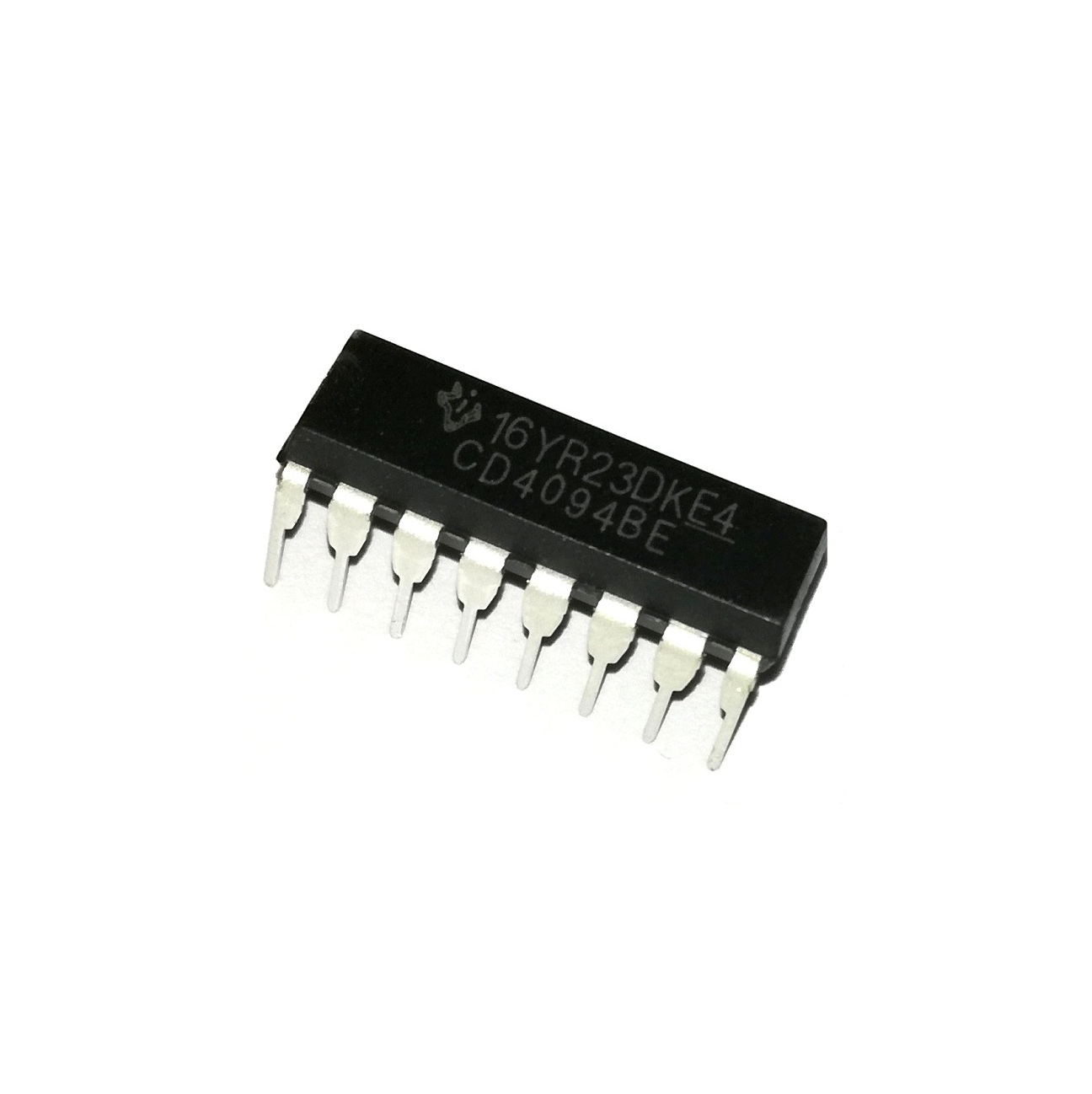
The CD4094BC consists of an 8-bit shift register and a 3-STATE 8-bit latch.Data is shifted serially through the shift register on the positive transition of the clock. The output of the last stage (QS) can be used to cascade several devices. Data on the QS output is transferred to a second output, Q¢S, on the following negative clock edge.The output of each stage of the shift register feeds a latch,which latches data on the negative edge of the STROBE input. When STROBE is HIGH, data propagates through the latch to 3-STATE output gates. These gates are enabled when OUTPUT ENABLE is taken HIGH.
Features
Question & Answer
Total 2 questions
Q: May I know the operating temperature of this product?? Questioned by Mithunagnik, 28-Jul-2017
Please see here. https://www.techshopbd.com/uploads/product_document/CD4094%20Datasheet.pdf Answered by A.R, 30-Jul-2017 16:51 PM
Q: I got it! and already ordered it.. Questioned by Mithunagnik, 30-Jul-2017
Reviews & Ratings
0 Ratings / 0 Reviews
Recently Viewed
Help: 09678110110
09.00am - 08.00pm (7 days a week)
Pay cash on delivery
Pay cash at your doorstep
Service
All over Bangladesh
Warranty and Replacement
Up to 1 Year