SHOPPING CART
PRODUCT CATEGORIES
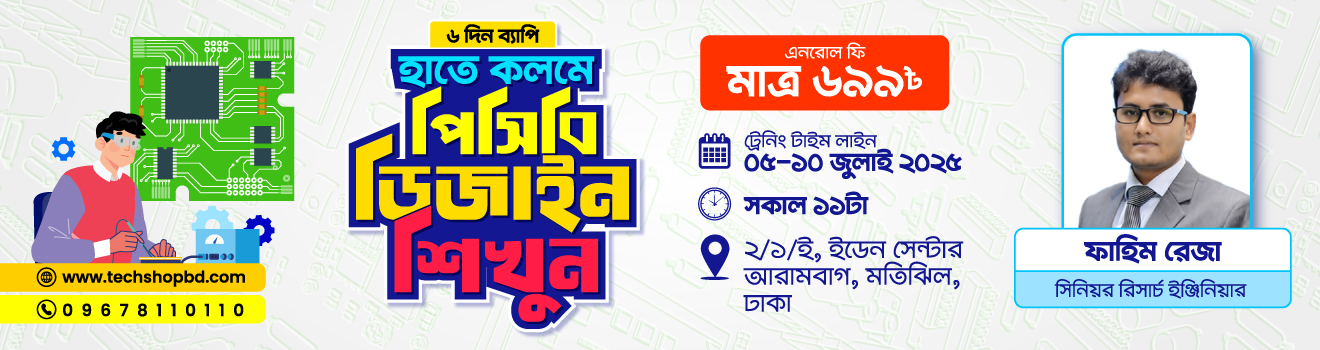
Type: Short Course
Duration: 6 Days
Time: 11:00 AM to 1:00 PM
Total Hours: 12 Hours
Location: 2/1/E, Eden Center, Motijheel, Dhaka. View Map
Do you want to participate? Join Now!
This Crash Course was designed to take you from mystery to Electronics and PCB Design mastery. This program covers both fundamental and advanced aspects of electronics, with a strong emphasis on hands-on experience using industry-standard tools.
People from any discipline with basic knowledge about electronics and the ability to follow along and build the circuits. No prior PCB design experience is required.
The course assessment will be conducted through individual assignments, quizzes, and a final examination. Participants will receive a certificate upon successful completion of the course.
Fahim Reza
Sr. Research Engineer
Pi Labs Bangladesh Ltd.
Pay cash at your doorstep
All over Bangladesh
Up to 1 year
Delivery Method
In Dhaka city and other divisional cities, home delivery is guaranteed. Currently, we are providing home delivery to 490+ upazilas across Bangladesh. However, in locations outside these areas, home delivery may be subject to availability based on whether the shipping address falls within the coverage zone of our partner courier service. If your address is outside the coverage area, you may be required to collect your product(s) from the nearest courier service office.
For further assistance and to confirm the delivery options for your location, please contact our customer care team at 09678 110 110.
Shopping Guideline
To purchase products from TechshopBD, you are required to create an account on our website, www.techshopbd.com. Once your account is set up, you can place orders by logging in. Please note that we do not accept orders through email, SMS, or phone calls, and we do not offer offline sales.
Shipping Options:
Courier Service: If you chose this option, your product(s) will be delivered by our partner courier service. If you shipping address is within Dhaka city (metro), you’ll get your product(s) in 2-3 working days. Outside Dhaka city, product(s) arrives in 3-5 working days.
Express Delivery:This service ensures that you’ll receive product(s) within 24 hours of placing order and is available only in Dhaka metro. Instead of courier service, we’ll send our own delivery man to your address. The delivery charge is a little bit higher than courier service but worth the extra expense if you’re in urgent need. Moreover, if you place order before 10 am, you’ll receive products on the same day, within 12 hours in most cases.
Order Status Tracking:
You can track all of your orders from the My Account > My Orders menu. When you place your order, it will go through a series of steps during fulfillment.
1. Processing: This indicates that we've received your order.
2. Verified : The order has been successfully verified by calling you.
2. Packaging : Your order is in the process of being prepared for shipment.
3. Shipped : Your order has been moved to our shipping dock. It's ready to go!.
4. Hold : This indicates your order needs human interaction before it can be released for shipment. Orders in this status usually get cleared quickly. We will contact you if we need additional information.
4. Cancel : This indicates that your order has been canceled. Orders may be canceled due to customer requests, payment issues, or other verification concerns. If you believe your order was canceled in error, please contact our support team for assistance.
6. Complete : Indicate that we have received the order amount from the payment channel.
Cancelling an Order:
If your order is in the Processing or Verified status, you can cancel your order by calling our hotline number (09678 110 110), which is available from 9 am to 8 pm. Outside this timeframe, as we’ll be unavailable, you can leave a message on customerservice@techshopbd.com. But due to normal variations in shipping speed, your order may have already been shipped by the time we get the message. If that is the case, it will not be possible to cancel your order. To avoid any trouble, please make sure you want everything in your cart before clicking on 'Place Order'.
Note: Please be advised that when an order is canceled, the cash refund process may take between 7 to 10 business days to complete.
Need Help?
If you have any questions related to orders and shipments, feel free to contact us.
E-mail: customerservice@techshopbd.com
Hotline: 09678 110 110 (9 am – 8 pm)
Payment Method
For payment, we offer two options: Cash on Delivery and Digital Payment (including bKash and other available methods).
If you choose Cash on Delivery, payment is due upon receipt of the product(s) from the delivery agent.
For Digital Payment, payment must be completed in advance. Once your payment is confirmed, we will process and dispatch your order for delivery.
Warranty Support
Please note that warranty claims made after the expiration of the warranty period will not be entertained.
Replacement WarrantyThe warranty will be void under the following circumstances:
TechShopBD reserves the right to modify or update any part of the warranty policy without prior notice.
Customer Support
At TechShopBD, we are dedicated to providing exceptional customer service to ensure a seamless experience for all our customers. Our support team is available from 9:00 AM to 8:00 PM, Saturday to Friday, to assist with any inquiries or issues you may have.
What We OfferIf you require assistance outside of our regular hours, please feel free to leave a message, and we will get back to you as soon as possible.